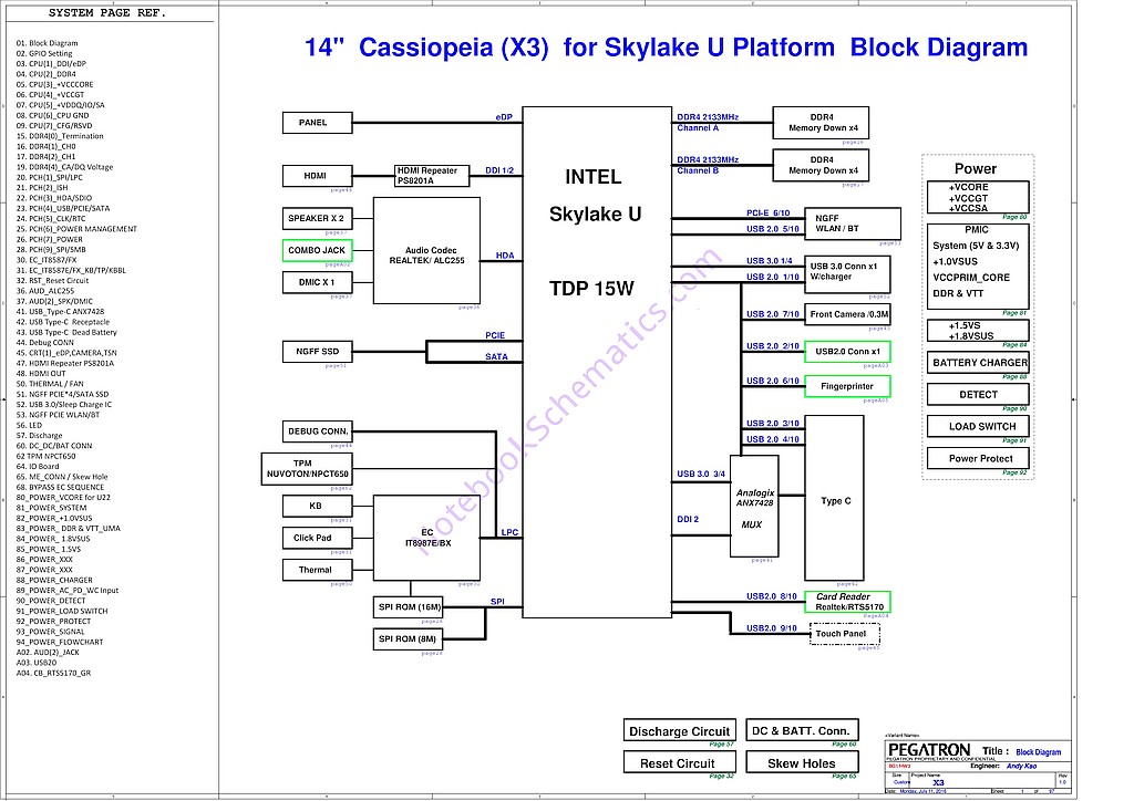
11+ Skylake Block Diagram PNG. Intel released technical documents that give us a peek into the die layout of this chip. Search and find more on vippng.
Acer Travelmate X349 M Series Schematic Pegatron Cassiopeia X3 Skylake Schematic Notebookschematics Com from notebookschematics.com
Although the skylake diagram is conceptual, it does allow you to understand how it the goal of sth is simply to help users find some information about server, storage and networking, building blocks. Parts of this section are mirrored in our separate motherboard overview. We have a die block diagram that shows everything really, the igpu space has increased heaps.
Follow their code on github.
Below is the block diagram of the skylake xeon d: Scalable design in haswell microarchitecture. Skylake is the codename used by intel for a processor microarchitecture that was launched in august 2015 succeeding the broadwell microarchitecture. Bom d vram x32 d.