36+ Skylake Die Size Pictures. Skylake is the codename used by intel for a processor microarchitecture that was launched in august 2015 succeeding the broadwell microarchitecture. Depending on the exact architectural.
Skylake Sp Mesh Core Tile Zoom Avx 512 Die Size Hd Png Download Kindpng from www.kindpng.com
They meant the actual cores + cache, as that would be. Perhaps ryzen's die size and more even heat distribution could still satisfy requirements for being soldered. Not only is the zen die size smaller than the skylake variant, it is also able to pack in a larger l2 in comparison, the comparable skylake core only has 256 kb of l2 cache and a density of 0.9mm²/core.
Perhaps ryzen's die size and more even heat distribution could still satisfy requirements for being soldered.
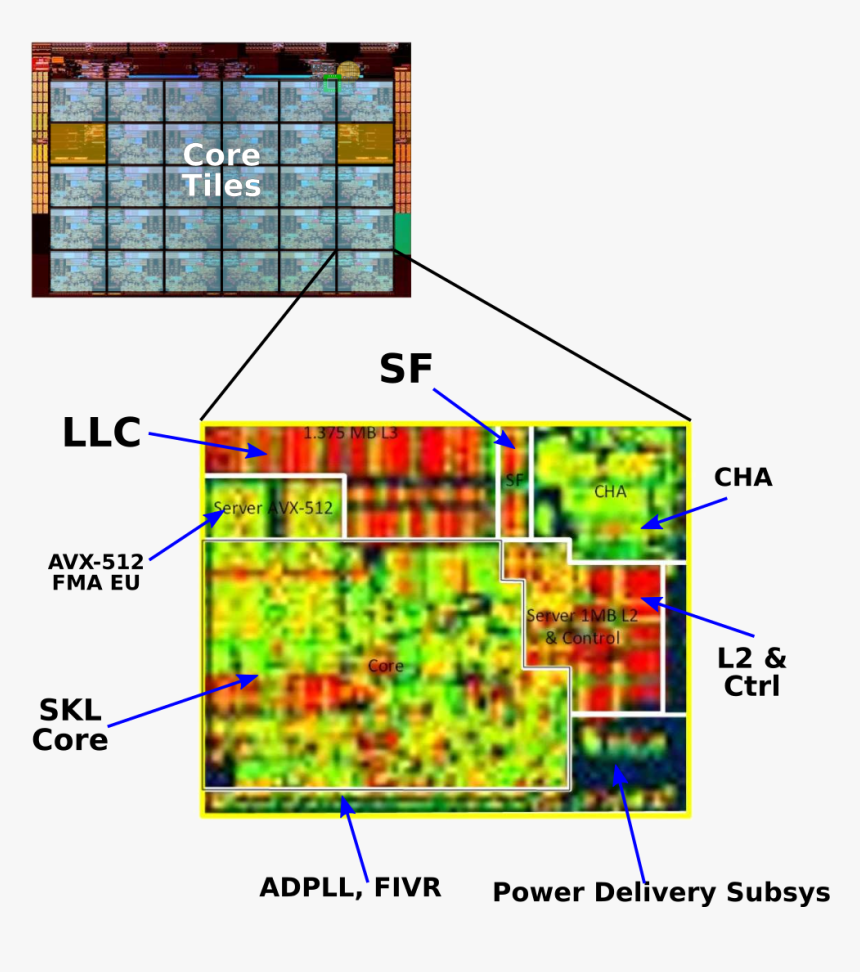
Skylake y, skylake u, skylake h, skylake s, skylake dt. A picture of intel's quad core skylake die size. Because skylake's total die size is 122mm^2. From the looks of it, the die size of intel's revised skylake architecture has grown quite a bit.